
A simple amplification circuit for analogue accelerometers
Published:
In my current work, I needed a solution to record audio frequency range vibrations using an accelerometer.
These would be recorded by a Teensy 4.0 microcontroller using one of its ADC inputs, then streamed to a host machine via USB audio.
I was using an ADXL1002 as it has a 10kHz bandwidth, but its ±50g range was a bit too large for my purposes.
The signal from the accelerometer therefore needed to be amplified before going into the Teensy’s ADC (as the ADC only has effectively 10 bits of usuable resolution, amplifying in the digital domain would be too noisy). Detailed here is the simple circuit I used for this purpose. None of this is ground breaking stuff, and just involves basic op-amp circuits (Douglas Self’s book “Small Signal Audio Design” is usually my go-to reference for this type of thing).
The Circuit
The basic circuit can be seen in the image below (note: the 100nF decoupling capacitors aren’t shown in this schematic - make sure that you use them next to each op-amp to go between the power supplies and ground). 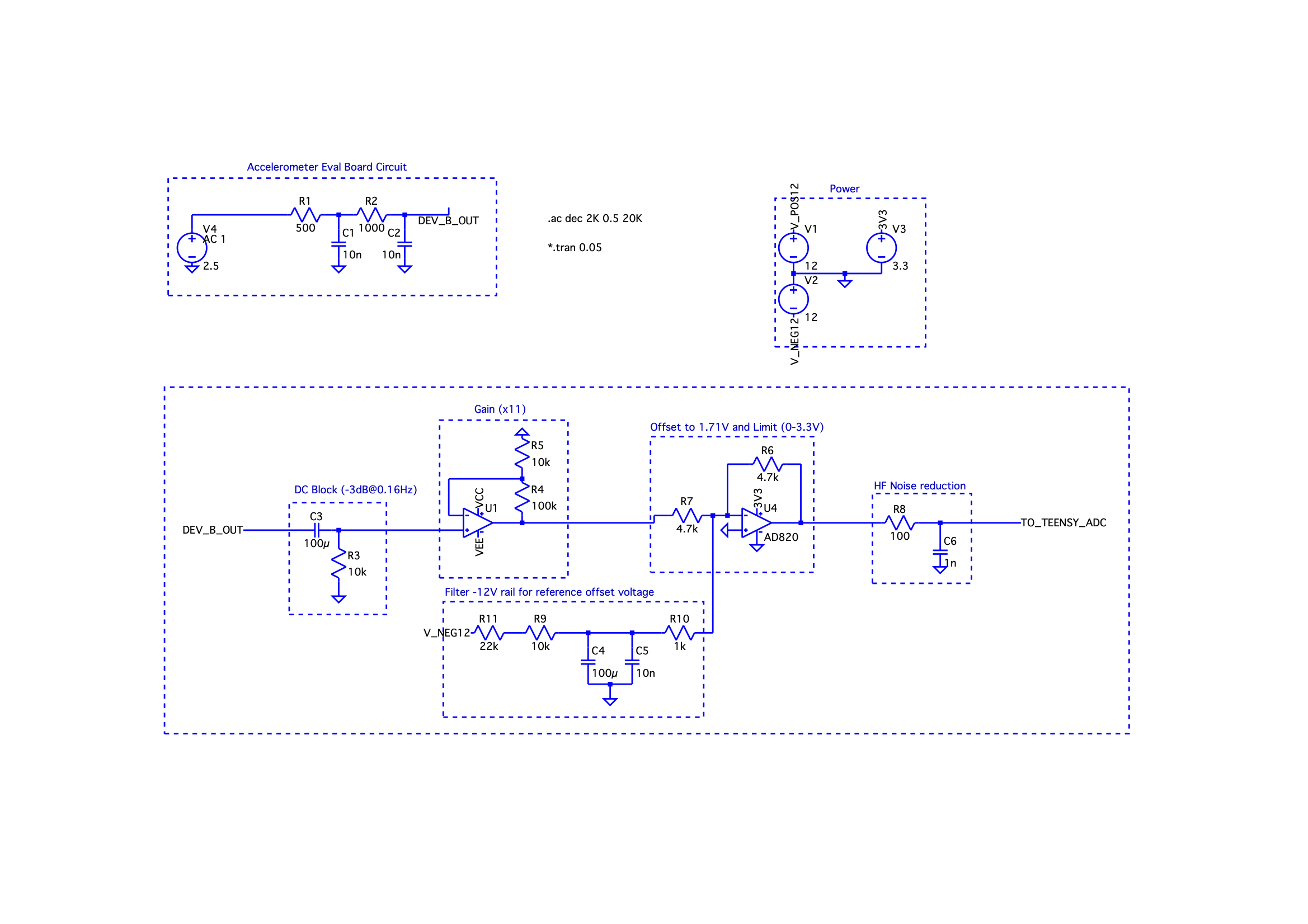
The eval board I was using had the resistor capacitor network shown in the top left already populated - this low-passes the accelerometer output at 10kHz.
For this circuit I was using a bench power supply to generate a -12V and +12V rail (using the 2 supply channels in series). I also used the fixed 5V output of the bench supply to power the accelerometer (it accepts power from 3V to 5.25V but a higher supply voltage gives more sensitivity). The 3.3V supply from the Teensy was used to power the second op-amp - more on this later.
DC Blocking
The accelerometer output has 0g as Vcc/2 - so 2.5V in out case.
We want to amplify the signal without amplifying the offset, so we need to get rid of this 2.5V offset. We could do this by using the same setup as described below - shifting the signal by -2.5V - but I didn’t need the signal to be DC coupled in this case so it was easier just to use a high pass filter with a very low cutoff frequency.
Amplification
The amplification stage used an NE5532 op-amp (powered from the ±12V supplies) in a classic non-inverting configuration with a gain of 11. This gain (calculated as (R4 + R5) / R5) is easily adjusted by changing the values of R4 and R5.
Offset and Limit
The most complex bit of this simple circuit is the offset and limit stage. In this stage, we need to offset the signal to centre roughly around 1.65V (as the Teensy’s ADC reads from 0 to 3.3V) and also makes sure that the signal never exceeds the 0-3.3V range.
Offset
To shift the signal, an inverting summing op-amp configuration is used. This sums the amplified accelerometer signal with a fixed voltage reference (taken from the -12V supply). We use a negative reference because the op-amp inverts the signal, so it will be a positive offset at the op-amp output. The amount of offset is determined by the resistor ratios (see the Wikipedia page for more info).
The -12V reference needed a 33k resistor to achieve a 1.71V offset (about as close to 1.65V as I could acheive with standard resistor values). To reduce noise from the voiltage rail, this is split into 32k of resistance, followed by two capacitors to ground, then the final 1k of resistance.
Limit
Limiting the output to between 0 and 3.3V is the easy part - all it requires is a rail-to-rail op-amp that can operate on 3.3V such as the MCP6004. The output of an op-amp will never exceed the supply rail voltages and therefore the signal is limited. This is the same idea that Thea Flowers explains in her excellent write up of the design of her synth modules.
High Frequency Noise Reduction
Finally, there is a resistor and capacitor to limit the coupling of digital noise into the signal, as recommended by PJRC (the makers of Teensy)> From their audio design tool docs:
“Noise coupling from digital circuitry inside the chip is always a problem when using ADC inputs pin. It’s never as quiet as the audio shield and any good quality audio ADC chip. Stong low impedance drive to the analog input pin is critical to minimizing noise coupling. If an opamp is used, connect a low value resistor (eg, 100 to 1000 ohms) between the opamp output and ADC input pin, and a 1nF capacitor from the ADC pin to GND or AGND. The capacitor lowers the impedance for high frequency noise, and most opamps require a resistor to avoid oscillation when driving a capacitive load. Strong drive from an opamp, 100 ohm resistor and 1nF capacitor can greatly reduce the digital noise coupling.”
Time Domain
Below you can see a time domain example from an LTspice simulation of a 200Hz sine with 0.05V amplitude feeding into the circuit, with the output also shown. 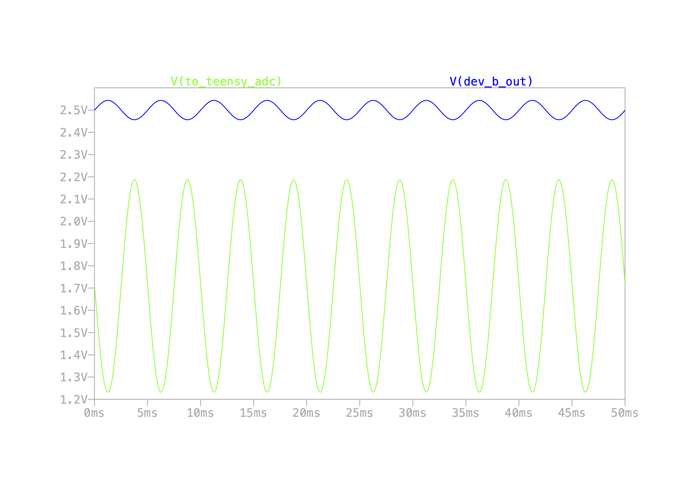
Frequency Domain
Here is the frequency domain response of the circuit - shown the DC blocking HPF, 10kHz LPF from the breakout board circuit, and overall system gain. 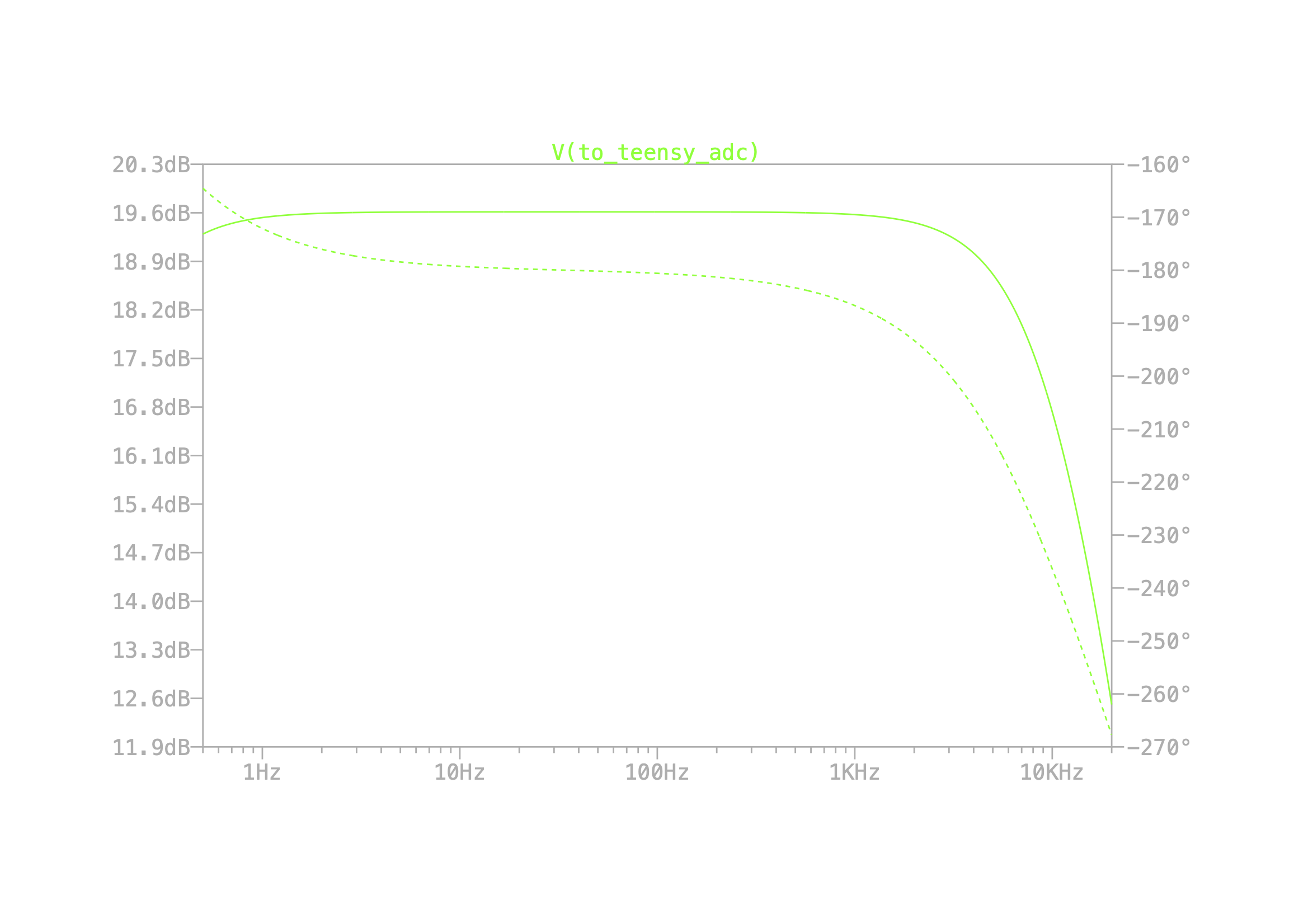
Conclusion
This is a really basic circuit - variants of which will have been done 1000s of times before, but I thought it might be useful for anyone needing a circuit of a similar purpose!
Remember, the output of this circuit will have the polarity inverted due to the inverting summing stage, but this is trivial to account for in software.
Finally, find the LTspice file here if you want to test it out for yourself.